
For decades, lithography has stood at the heart of semiconductor advancement. It enabled Moore’s Law by shrinking transistors with predictable precision, and its progress was measured by nanometers and numerical apertures. But as we move into the next generation of chipmaking, where improvements come from multidimensional scaling, advanced packaging, and cross-domain integration, the language used to describe progress is becoming outdated. Erik Hosler, a strategist who bridges consumer expectations with advanced semiconductor ecosystems, points out that the industry’s vocabulary is no longer aligned with what truly matters.
Semiconductor marketing and engineering teams are beginning to reckon with the reality that consumers and even many enterprise buyers do not think in nanometers or care about pitch resolution. They think in terms of device performance, battery life, and seamless user experience. If next-gen lithography is to capture imagination and investment, it needs to adopt a language that reflects today’s broader development context, one that communicates value beyond shrinking features.
A Legacy of Metrics
For much of the industry’s history, lithographic advancement was expressed through a simple metric: the minimum feature size. From 130 nm down to 5 nm, these numbers signaled progress, competitiveness, and capability. A smaller number meant more transistors, better performance, and often, industry leadership.
It worked well in the era of planar scaling. Feature size reductions directly translated to power and performance improvements. It was a language the entire industry, from engineers to Wall Street analysts, could understand.
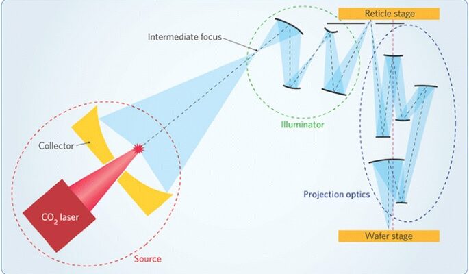
But that simplicity is fading. Today’s most advanced nodes rely on complex processes like multi-patterning, EUV, 3D stacking, and chiplet integration. These do not scale linearly and cannot be captured accurately by a single number. Yet, we still describe them using terms rooted in a different era.
The Disconnect Between Words and Value
As lithography advances, the language used to describe it becomes more abstract. Consumers hear terms like “EUV,” “0.55 NA,” or “multi-patterning,” but without a clear connection to benefit. Even seasoned technologists struggle to interpret what a process name like “3 nm class” implies, especially when definitions vary by manufacturer.
This linguistic gap creates confusion not just for the public but also within the supply chain. Designers, tool vendors, and material suppliers often operate with different assumptions about what a node name represents. As development spreads across more dimensions, a single metric can no longer convey advancement. In short, the current language is failing to reflect the complexity and opportunity of modern lithographic strategies.
From Feature Size to Functional Impact
The time has come to shift from discussing transistor width to discussing function. Instead of communicating progress through physical attributes, the industry can emphasize performance-per-watt, system-level gains, AI responsiveness, and workload optimization.
Erik Hosler notes, “This is because consumers don’t care what the feature size is inside a chip.” That statement reflects a fundamental truth. Consumers care about what a chip enables, not how it was made. They notice whether their devices are faster, more responsive, or better at managing power, not whether a chip was built at 3 nm or 5 nm. By redefining how we talk about progress, the industry can better align with end-user priorities and future-proof its messaging.
Lessons from Other Domains
Other sectors have already made this linguistic leap. In automotive technology, the conversation has moved from horsepower and engine size to safety features, infotainment systems, and range. In photography, megapixels are now secondary to image processing and real-time enhancements.
Semiconductors can do the same. Instead of focusing exclusively on geometric scaling, the narrative can embrace the integration of photonics, the role of AI in design and manufacturing, and the benefits of system-in-package solutions. These are the dimensions of innovation that can define the future, and they deserve to be communicated in ways people can relate to.
Toward a Multivariable Lexicon
Rather than replacing one metric with another, the industry should consider adopting a multivariable language, one that includes several dimensions of progress. These could include:
- Energy Efficiency: Performance per watt across real-world workloads
- Integration Density: Functionality per unit area, including chiplets and stacked elements
- AI Capability: On-device intelligence, throughput, and responsiveness
- Security and Reliability: Hardware-level features that enhance trust and durability
- Manufacturing Flexibility: Adaptability to different process flows or materials
Together, these metrics provide a richer picture of what modern lithography enables. That also shifts the focus away from how small we can go and toward how much we can achieve.
The Role of Marketing and Communication
Engineers cannot make this shift alone. The move to a new language requires marketing teams, analysts, and media to buy into the change. It means designing product launches, keynote presentations, and investor communications around experiential gains rather than process nodes.
It also means being more transparent about what modern technology does well and what tradeoffs it brings. For instance, moving to high-NA EUV might improve resolution but require more complex optics and higher costs. Explaining these dynamics in plain terms builds credibility and invites more nuanced discussions. With the right communication strategy, advanced lithography can become not just a technical marvel but a compelling story about innovation that matters.
Educational Responsibility
Part of building a new language involves education. Semiconductor companies and research institutions can help shape how the next generation of technologists and customers understand progress. It includes updating internal training, rethinking external messaging, and collaborating with partners to align vocabulary across the ecosystem. A shared language makes it easier to collaborate, develop, and build trust.
This responsibility also extends to public discourse. As chips become more integral to every facet of life, explaining their advancement in accessible terms helps demystify the technology and foster informed conversations.
Rethinking What Progress Sounds Like
Next-gen lithography is more capable than ever, but its complexity is masked by outdated terminology. As we move deeper into a world shaped by advanced integration, cross-disciplinary engineering, and application-driven design, the language of chipmaking must develop.
That development begins by recognizing that transistor size is no longer the sole or even primary indicator of value. It continues with the adoption of terms that reflect real-world performance, adaptability, and user-centric gains.
Moore’s Law may have started with a number, but its future depends on a narrative. If the semiconductor industry hopes to lead the next era of development, it must find words that reflect not just where we are going but why it matters when we get there.